Lock Box Project
PHYS 352 – Electronics II
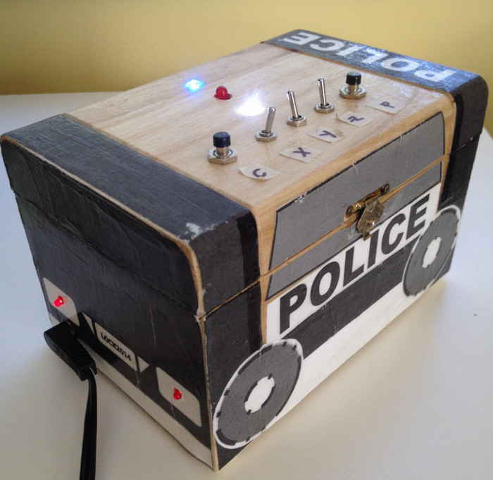
Designed circuit with five input controls (switches and pushbuttons), three LEDs, fiber optics, buzzer, and fan. Developed three stages using digital electronics: logic gates, one shot, shift register, demultiplexer, counter, and SR latch. Simulated circuit in MultiSim. Tested on breadboard. Soldered and packaged final product. Utilized feedback and sequential logic to ensure stages must be unlocked in order. Forced stage reset upon incorrect timing or sequence. Indicated stage completion with LEDs.
Circuitry Design
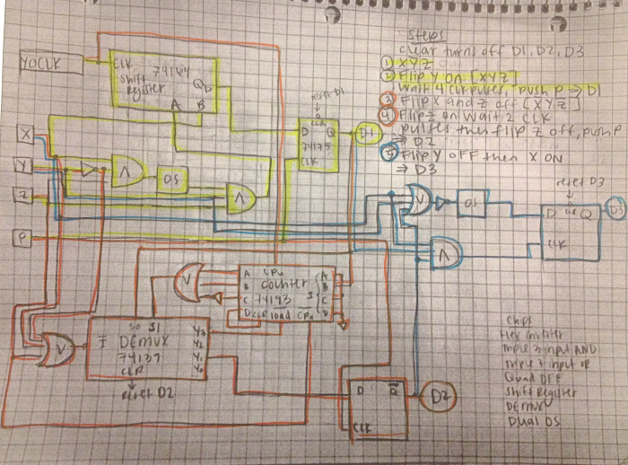
When trying to simulate the lock in MultiSim, I realized that the push-button was way too short of a pulse to be used as it was designed in the working design. Additionally, I didn’t realize how huge the timing delay is on MultiSim, but eventually I figured it out. (Hence the 20Hz YOCLK pulse…I plan on actually using an ~1Hz YOCLK. I’m also going to change the timing delay of the One Shots to ~0.5 sec.) The way the lock is shown, the final LED does not turn off unless the power is turned off, but I am going to try to rework that portion as well as trying to remove a logic gate in the first stage.
 |
 |
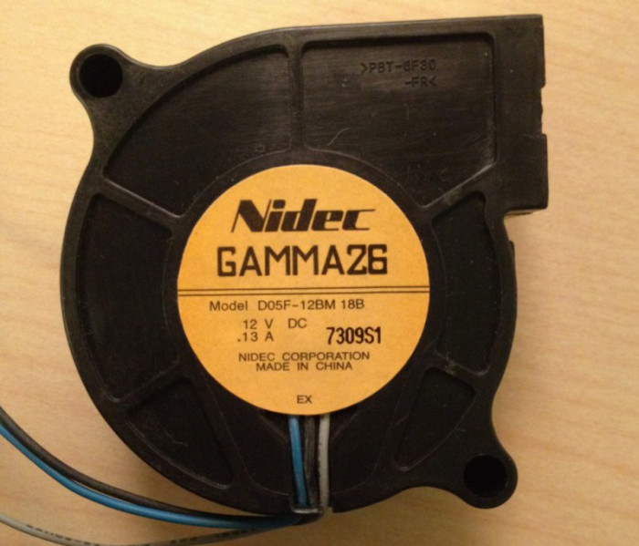 |
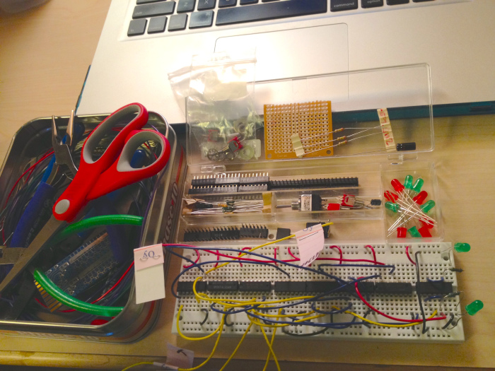
| Hand-Drawn Circuitry | Supplies | Moving Element: http://youtu.be/8beHugblAtk |
Breadboard Testing
Stage 1: Below is a video of the functioning first stage of the lock. I was having an issue with the One Shot (OS) chip triggering on both positive and negative edges, so I replaced it with a 556 monostable multivibrator circuit (another name for a OS). Also, the SR Latch replaced the DFF to allow the use of a single chip (rather than 2 DFF chips as needed by the original design). Below the picture is the link to a video which shows the first stage in action! As desired, D1 (Green LED) turns off when the clear button is pushed. This step used the X, Y, and Z switches as well as the YOCLK.
Stage 2: Below is a video of the functioning second stage of the lock. I replaced the 74139 DEMUX from the original schematic with the 74138 DEMUX. This forced D1 to be HIGH before the second stage can be enabled via the DEMUX. Additionally, it made the logic less repetitive and removed the need for one of the logic gates. Again, the SR Latch replaced the DFF to allow the use of a single chip (rather than 2 DFF chips as needed by the original design). Below the picture is the link to a video which shows the second stage in action! As desired, D2 (Green LED) turns off when the clear button is pushed. This step used the X, Y, and Z switches, the P pushbutton, and the YOCLK.
Stage 3: Below is a video of the functioning third stage of the lock. As with the first stage, the One Shot (OS) chip was replaced with one constructed with a 556. The clear for the OS was also replaced with the Y to ensure desired logic was followed. (Once again, the SR latch replaced the DFF.) Below the picture is the link to a video which shows the third stage in action! As desired, D3 (Green LED) turns off when the clear button is pushed. This step only used X and Y.
Soldering
| Chips Used | Color Key, TOP | Color Key, BOTTOM (not shown) |
|---|---|---|
| N555N [YOCLK] | Blue = Stage 1 | Black = GND |
| SN74LS04N [Inverter] | White = Stage 2 | White = Clear |
| SN74LS11N [And] | Brown = Stage 3 | Brown = P |
| 74HCT4075N [Or] | Orange = YOCLK | Red = Vcc (+5V) |
| NE556N [One Shot] | Yellow = X | |
| 74HCT164N [Shift Register] | Green = Y | |
| 74HCT138 [Demultiplexer] | Purple = Z | |
| SN74LS193N [Counter] | Red = Clear | |
| SN74LS279N [SR Latch] |
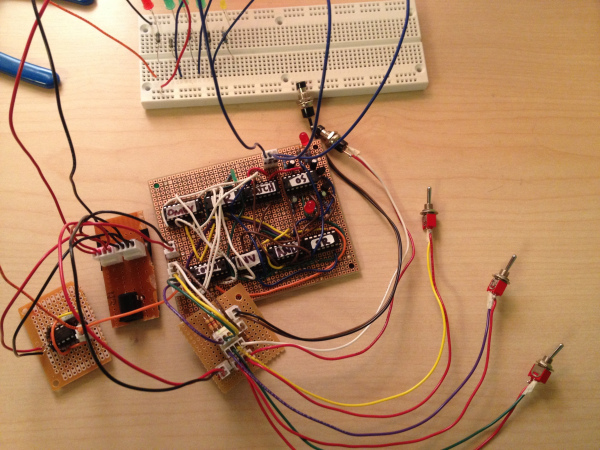 |
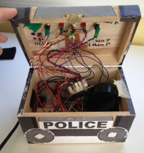 |
| Circuitry prior to install | Circuitry inside the Box |
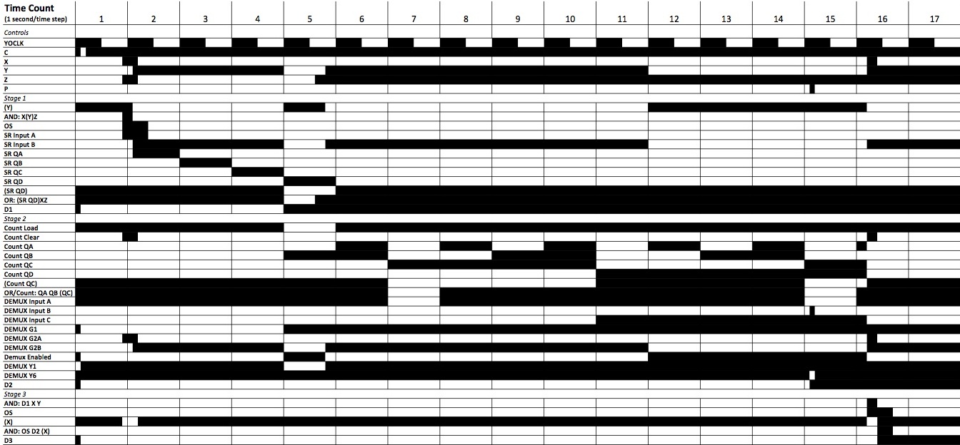
Timelines
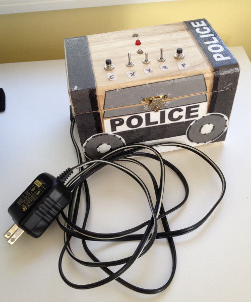
Finished Product
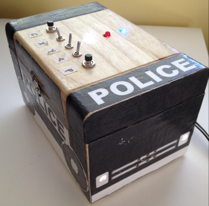 |
 |
YOCLK & LabVIEW Controls
The lock operates based on an oscillating clock called “YOCLK”. The schematics of the lock as well as a video can be found here. A LabVIEW program was created to be able to control and unlock the Lock Box called LockTest.vi.
